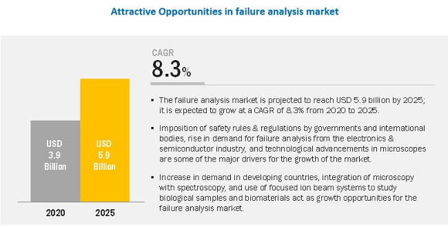
The failure analysis market is estimated to be valued at USD 3.9 billion in 2020 and is projected to reach USD 5.9 billion by 2025; it is expected to grow at a CAGR of 8.3% from 2020 to 2025. A few key factors driving the growth of this market include imposition of safety rules & regulations by governments and international bodies, rise in demand for failure analysis from the electronics & semiconductor industry, technological advancements in microscopes, and rising focus on nanotechnology and regenerative medicine.
Download PDF Brochure:
https://www.marketsandmarkets.com/pdfdownloadNew.asp?id=149011970

The Focused Ion Beam (FIB) system market is expected to grow at the highest CAGR during the forecast period. FIBs are primarily used for semiconductor manufacturing. The development of commercially focused FIBs has led to their increased applications in the field of material sciences. In addition to circuit editing and Transmission Electron Microscopy (TEM) sample preparation, FIBs can now be used for microstructural analysis and prototyping nanomachining. The fastest growth of this segment can be attributed to the growing adoption of FIB systems in material science and bioscience applications.
The failure analysis market for Focused Ion Beam(FIB) technology is expected to grow at the highest CAGR during the forecast period. Exponential growth has been observed in research activities related to material science across the globe. Research activities require sophisticated analytical tools to analyze and understand new materials that possess prominent physical properties. FIB technology offers both analytical and patterning capabilities in a single instrument.
The failure analysis market for material science application is expected to grow at the highest CAGR during the forecast period. This is due to the high adoption of failure analysis equipment for material science applications. In material science, Focused Ion Beam (FIB) systems and dual beam systems are used as a sample preparation tool and a microscope for micro- and nanosectioning processes, site-specific transmission electronics microscope(TEM) sample preparation, deposition, and polishing of materials as well as their manipulation.Microscopes are used for the structural and chemical analysis of materials, including polymers, metals, alloys, ceramics, and biomaterials.Optical microscopy and scanning electron microscope (SEM) are standard techniques in mineralogical and structural investigations of geological and archaeological samples.
Get in-depth analysis of the COVID-19 impact on the Failure Analysis Market
Request Free Sample Report:
https://www.marketsandmarkets.com/requestsampleNew.asp?id=149011970
The failure analysis market in APAC is expected to grow at the highest CAGR during the forecast period.The rising R&D funding for microscopy research, increasing application of correlative microscopy in life science and nanotechnology research,mass production of electronic products such as smartphones, tablets, sensors, industrial equipment, wearables, and white goods in China and Taiwan is expected to accelerate the growth of the failure analysis market in the region.
The major opportunities for the growth of failure analysis market include increasing demand for failure analysis in developing countries, integration of microscopy with spectroscopy, and use of Focused Ion Beam (FIB) systems to study biological samples and biomaterials.